

Optimizing InGaN templates for LEDs
North Carolina State University has been investigating the potential of indium gallium nitride (InGaN) for enhancing the performance of III-nitride light-emitting diodes (LEDs)
March 15, 2022 ![]() Isabella Mormando
Isabella Mormando
Salah Bedair, ECE Distinguished Professor, and his research team have been investigating the potential of indium gallium nitride (InGaN) for enhancing the performance of III-nitride light-emitting diodes (LEDs) [Mostafa Abdelhamid et al, Appl. Phys. Lett., v120, p081104, 2022].
The reduced strain in InGaN quantum wells (QWs) grown on InGaN templates should increase light output, particularly for the longer wavelengths desired in micro-LEDs and full-color displays – but there is a trade-off since such templates have higher defect densities relative to pure GaN. For commercial use, the former effect must significantly outweigh the latter. The balance arises through the strain effects of lattice and thermal expansion mismatching between GaN and the target InGaN. Using an intermediate InGaN template should lighten these constraints.
The team used commercial substrates with 5μm n-GaN on sapphire with ~108/cm3 dislocation density to grow InGaN QWs on InGaN templates (Figure 1). The researchers employed their own metal-organic chemical vapor deposition (MOCVD) system with substrates rotating under alternating streams of III and V precursors.

Figure 1: Schematic of (a) conventional LED on GaN (LEDGaN), and (b) LED on InGaN SB template (LEDSB).
The main precursors were trimethyl-In/Ga for the group-III metals and ammonia (NH3) for the group-V nitrogen. However, the QWs were grown with triethyl- rather than trimethyl-Ga.
The ~600nm InGaN template was produced using what the researchers call a semi-bulk (SB) approach where 30-periods of 20nm InGaN layers were separated by 2-4nm GaN caps. These thicknesses gave optimized surface morphology with reduced V-pit size and depth, according to research by the team and others.
The effective indium content varied according to growth temperature. The template indium contents were in the range 8-12% (Table 1). The researchers comment: “We define the effective indium content as the reduced indium content value that corresponds to full relaxation in the top layers of the SB templates. For example, a template with an indium content of 10% that is 85% relaxed is equivalent to a fully relaxed template with an effective indium content of 8.5%.”
Table 1:
| LED | SB1 | SB2 | SB3 | SB4 |
| Temperature |
745°C |
740°C |
735°C |
730°C |
| In content | 8.5% | 9% | 10.5% | 11% |
The QWs grown on the template at 710°C were capped with 1nm aluminium gallium nitride (Al0.25Ga0.75N), presumably to reduce decomposition of the InGaN layer during the 100°C higher temperature GaN growth. The use of triethyl-Ga with very low molar flow (0.78μmol/min compared with 3μmol/min for conventional wells) reduced indium incorporation to give similar wavelength performance (~475nm) across the different templates studied. The p-GaN contact layer was grown at 975°C.
Both the conventional and template materials used high-temperature (HT) SB layers before the QWs. These consisted of In0.05Ga0.95N layers grown at 770°C. These layers were used to “improve the electron injection into the active region and slightly reduce the strain in the wells”. The HTSB also improves surface morphology for the QW growth. An HTSB section was also inserted in the template layer with a view to further reducing defects.
The material was fabricated into 400μm x 400μm LEDs. While the LEDSB1 and LEDSB2 devices showed enhanced light output power and external quantum efficiency (EQE) over the conventional LED, the higher-indium-content templates showed degraded performance (Figure 2). In fact, the degradation was monotonic so that the performance of LEDSB1 was better than that of LEDSB2, while both were better than the conventional device (LEDGaN). The peak EQE of LEDSB1 was about 1.9x higher than LEDGaN.
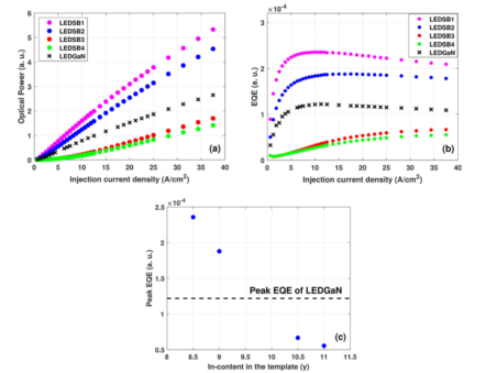
Figure 2: Comparison of (a) optical power measurements and (b) relative EQE for LEDGaN and LEDSB1-LEDSB4. (c) Peak EQE versus indium content in underlying template. Horizontal line shows peak of LEDGaN.
Bedair and his research team attribute the improvements over the conventional LED to reduced electrical fields in the active region. These electric fields arise from the charge polarization of the III-V chemical bonds leading to strain-dependent effects. When electric fields are present in the active regions they tend to inhibit electron-hole recombination into photons, what researchers often describe as the ‘quantum-confined Stark effect’, or QCSE.
The degradation with increased indium-content templates is attributed to increased surface roughness, and deeper, wider V-pits.
The team summarizes: “There are optimum indium-content values in the template where the improvement due to the reduction in the strain is stronger than the deterioration added by the increased surface roughness and increased defect density.”
The lower-indium-content template LEDs also showed reduced saturation current under reverse bias, again indicating reduced defect density.